Can anyone explain how you go about building your own PC boards? I'm curious as to how people building their own stuff from scratch go about it.
For example:
How do you do component layout?
There are different ways to to this, right, you can do a photographic board from a positive or negative and you can also do CNC, correct? I imagine CNC units are pricey enough to only be in the hands of pros, right? Can you do photo-based stuff at home?
How do you drill holes? Just real carefully by hand?
Thanks, and sorry for the dumb questions
Printed Circuit Boards
-
The Scum
- moves faders with mind
- Posts: 2746
- Joined: Thu Jul 03, 2003 11:26 pm
- Location: Denver, CO
- Contact:
In the old days, people drew on film with markers and used that to make the necessary film to expose a PCB. Look at old Neve or API cards, and the traces on them have a very flowing, organic quality, because they were drawn by hand.How do you do component layout?
Today, in 2006, I use software for my layout. I use a pacakge called Eagle, from www.cadsofe.de. There's a free version you can experiement with. You start by entering the schematic for what you're building. Then you change modes, and it gives you the schematic components, bound together with rubber-band lines. You arrange the components, then turn the rubber-band lines into traces. Getting into Eagle the first time is a little daunting, it's a very complicated program, but the nuance it allows is actually very useful...it'll protect you from making a board layout that doesn't match your schematic!
There are also SPICE programs that'll read your Eagle schem and let you simulate it.
There are other PCB programs out there...I used to use the free DOS version of Easytrax or whatever it was from Protel. The way it scrolled used to make me seasick, and it was actually pretty hard to make a nice board with it. Eagle is FAR superior!
There is photo-based stuff you can do at home. There's also a little more home-friendly process using a laser printer/toner transfer method that's not so bad. A web search for "Press-n-peel blue" should turn up some good reading.There are different ways to to this, right, you can do a photographic board from a positive or negative and you can also do CNC, correct? I imagine CNC units are pricey enough to only be in the hands of pros, right? Can you do photo-based stuff at home?
I've never seen a CNC trace-cutting setup that was affordable to the
hobbyist.
A drill press is highly recommended. You'll need special bits to do it...I think they're carbide, but I could be mistaken. The fiberglass in the board will ruin ordinary bits very quickly.How do you drill holes? Just real carefully by hand?
I have seen plans for a DIY CNC drill machine...a small one wouldn't be too tough to cconjure.
As for actually etching my own PC boards, I haven't done it in a long time. It's a tedious process involving some pretty nasty chemicals...and it's a lot of work to make a board that's mediocre at best. If you're doing double-sided work, you can't to the through-hole-plating in your own.
My advice: If you're only making one of something, do it on perfboard. If you want to make a handful of it, spend your time with the layout to get it right. Then send out to have it fabbed elsewhere. I get a better board than I can make at home, often quicker than my DIY time budget would allow, and the quality & convenience more than make up the price difference.
I've used www.4pcb.com many times now...they offer some specials for DIYers. Look into the bare-bones and 3 for $100 services. Not 10 minutes ago, my latest boards arrived from them...and I placed the order 3 days ago.
I've also used olimex.com a couple times. Their prices are great, but having to fax stuff to Bulgaria was a bit of a hassle.
There are many other companies, check your yellow pages.
Byron Jacquot
I think Byron's comments are very good.
I'll add that I think it's quite easy and inexpensive to make boards at home once you get the hang of it. You can buy an optical printing kit from GC that has developer, etchant, an agitation tub and a couple of presensitized boards.
You don't have to buy and/or learn a fancy electronics design package to make layouts. They're kindof indispensible if you're going to send them out to have them professionally made since you need your layout to be in one of a few specific file formats, but it's not necessary, and in fact in my opinion it's often preferrable to do it "by hand". I routinely make board layouts with Photoshop, and have seen nice layouts that were done in microsoft paint.
I like to use the GC presensitized boards. You just print your image on transparency, lay it on top of the board, expose it to sunlight for a few minutes, stick it in developer for a minute or two, and etch it. Once you do one or two it becomes super easy, enough so that I often do it for one off boards.
You can print the layout on transparency film on your home laser printer, but I'll warn you that I find it best to make two copies and very carefully glue them together so they're precisely aligned. Otherwise the black isn't dense enough to keep out light and you can get messy partially etched lands.
I think it's best to expose the GC boards in shade or under overcast sky, not direct sunlight, for about 5 minutes. Direct sunlight works too fast and if your timing isn't precise you can get bad results. Shade is slower and the timing doesn't have to be as exact. If you're just doing a board every now and then I don't think you need to buy a special controlled UV chamber, although some people will tell you should. The shade is pretty reliable.
I used to drill with a press, but it took a long time. These days I just use a dremel. Dremel makes a kit of tiny drill bits that work. They last pretty well actually, particularly if you dip them in wd-40 between every couple holes. I probably drill a few hundred holes with a bit, but yes, they eventually dull. Also, if you happen to do it this way, be sure you don't let the tip of the bit extend more then half a cm or so outside the chuck. Otherwise you'll snap the bit off for sure.
With home printing your resolution isn't great and your hand drilling accuracy won't be totally accurate. For this reason you'll want to be sure to make your traces and pads fairly large, and leave reasonable space between them. This is another good reason to forgo the autocad type board layout tools. You can't cram as much junk on the board, but if you're doing it at home that's not really an option anyway.
Ned
-
blakbeltjonez
- gimme a little kick & snare
- Posts: 83
- Joined: Sat Feb 12, 2005 3:00 pm
- Location: florida
thanks for the GC tips, nclayton.... i have had trouble with the GC stuff, very erratic results.
if you need tiny drill bits cheap you can get various sizes (3/64 on down) from welding supply shops - just ask for welding tip cleaners and you get an aluminum pen-type tube with screw-off top of about a dozen for $10 or so. perfect for PCB drilling, and to find elsewhere can be difficult (i've only really seen small bits at hobby shops) and often quite a bit more expensive.
if you need tiny drill bits cheap you can get various sizes (3/64 on down) from welding supply shops - just ask for welding tip cleaners and you get an aluminum pen-type tube with screw-off top of about a dozen for $10 or so. perfect for PCB drilling, and to find elsewhere can be difficult (i've only really seen small bits at hobby shops) and often quite a bit more expensive.
Once Upon A Time, I laid out many circuit boards in the "pre computer" era.
Vendors such as Bishop Graphics (unfortunately, out of business) and others sold a variety of "sticky" pieces such as round "donuts" for mounting through-hole resistors and capacitors, pre-spaced "stickies" for IC sockets, etc. To tie them together, they also sold rolls of thin mylar or crepe tape.
I had a light table (plate glass atop a white difussor plastic with fluorescent bulbs beneath). On top of the glass, I taped a translucent mylar sheet with a grid pattern with lines on 0.1" centers (another Bishop Graphics item). On top of THAT I taped a clear sheet of mylar.
On that clear mylar, I'd then apply the various "stickies", using the underlying grid for locating the parts, and then tying them together with the thin strips of mylar or crepe tape.
Bishop sold "stickies" in 1:1, 2:1 or 4:1 sizing. I used 2:1.
When I was finished, I sent the mylar with all of the stickies to someone with a litho camera and had them shoot film at 50% size.
I was actually pretty good at it. <g>
Nowadays very few PC board companies can accept film artwork. FARcircuits still uses that process.
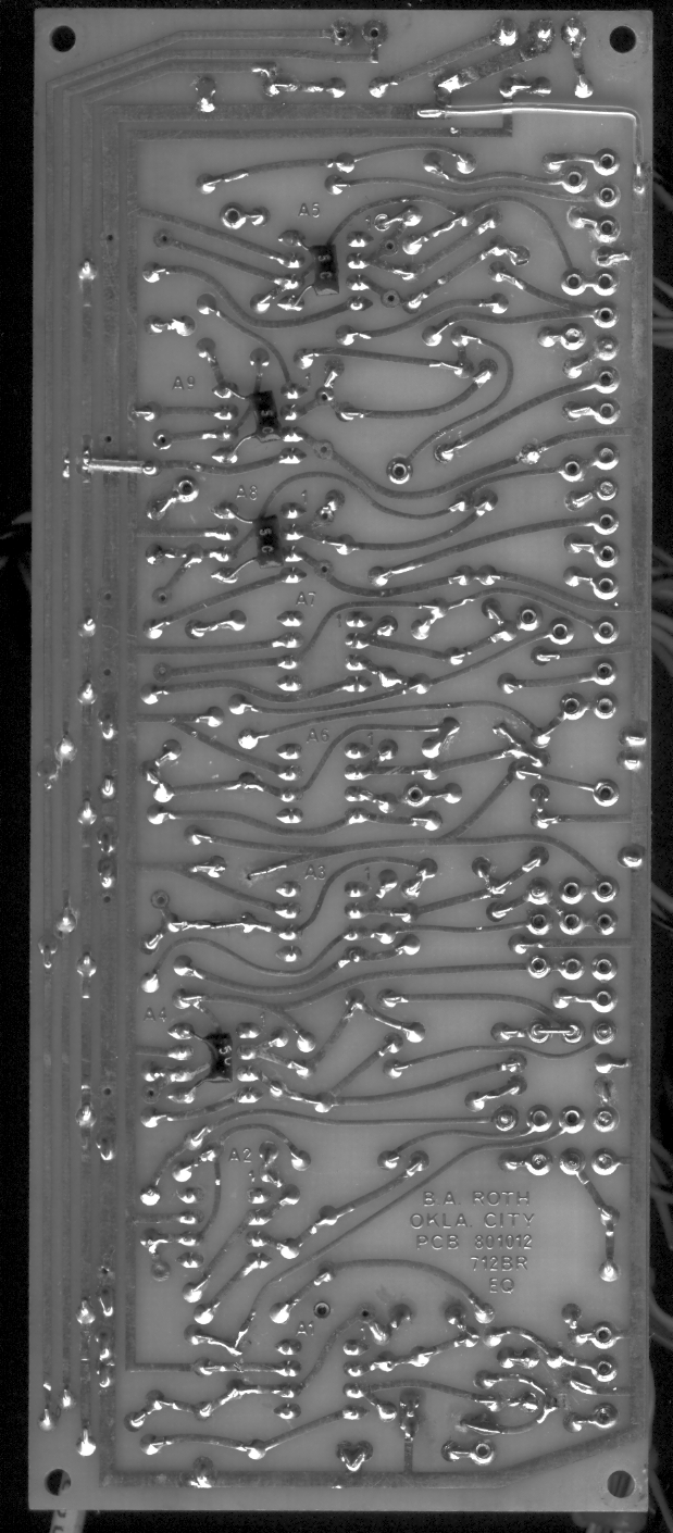
EDIT. I realized I had placed the EQ board from the console I built in 1977 onto my scanner awhile back:
http://www.brianroth.com/pix/eq-pcb.png
You can see how it all worked out, with the "donuts" and pre-spaced pads for the IC sockets and the "crepe" tape for interconnections. You can also see a few "fixes" on the foil side... capacitors and a jumper or two <g>
It was laid out as I described .. 2X..then shot at 50% onto litho film.
"Film at 11:00" here, in case anyone is interested about the project:
http://www.brianroth.com/projects/m77/m77.html
It was definitely a case of being in over my head for a DIY project..LOL!!!
Bri
Vendors such as Bishop Graphics (unfortunately, out of business) and others sold a variety of "sticky" pieces such as round "donuts" for mounting through-hole resistors and capacitors, pre-spaced "stickies" for IC sockets, etc. To tie them together, they also sold rolls of thin mylar or crepe tape.
I had a light table (plate glass atop a white difussor plastic with fluorescent bulbs beneath). On top of the glass, I taped a translucent mylar sheet with a grid pattern with lines on 0.1" centers (another Bishop Graphics item). On top of THAT I taped a clear sheet of mylar.
On that clear mylar, I'd then apply the various "stickies", using the underlying grid for locating the parts, and then tying them together with the thin strips of mylar or crepe tape.
Bishop sold "stickies" in 1:1, 2:1 or 4:1 sizing. I used 2:1.
When I was finished, I sent the mylar with all of the stickies to someone with a litho camera and had them shoot film at 50% size.
I was actually pretty good at it. <g>
Nowadays very few PC board companies can accept film artwork. FARcircuits still uses that process.
EDIT. I realized I had placed the EQ board from the console I built in 1977 onto my scanner awhile back:
http://www.brianroth.com/pix/eq-pcb.png
You can see how it all worked out, with the "donuts" and pre-spaced pads for the IC sockets and the "crepe" tape for interconnections. You can also see a few "fixes" on the foil side... capacitors and a jumper or two <g>
It was laid out as I described .. 2X..then shot at 50% onto litho film.
"Film at 11:00" here, in case anyone is interested about the project:
http://www.brianroth.com/projects/m77/m77.html
It was definitely a case of being in over my head for a DIY project..LOL!!!
Bri
-
moosapotamus

- gimme a little kick & snare
- Posts: 96
- Joined: Thu Feb 26, 2004 12:18 pm
- Location: New Hampshire, USA
- Contact:
Re: Printed Circuit Boards
As someone already mentioned, I would also recommend using Press-n-Peel Blue if you want to etch your own PCBs. There's a couple nice photo essays of how to do it at tonepad.com. Also, smallbearelec.com sells PnP by the sheet.ckeene wrote:Can anyone explain how you go about building your own PC boards? I'm curious as to how people building their own stuff from scratch go about it.
For example:
How do you do component layout?
There are different ways to to this, right, you can do a photographic board from a positive or negative and you can also do CNC, correct? I imagine CNC units are pricey enough to only be in the hands of pros, right? Can you do photo-based stuff at home?
How do you drill holes? Just real carefully by hand?
Thanks, and sorry for the dumb questions
As for drilling the holes, I don't have a drill press. So, I start with a spring-loaded center-punch to make a nice little dimple that keeps the drill bit from skidding around. Then I use a dremmel to drill out all the holes. I think the bits I have are 0.040".
I'm hooked on ExpressPCB for doing schematics and PCB layouts. The software is free and really easy to use, especially if you take 5 minutes to read the quick start guide. You can also use the software to order PCBs of your layout from them. It's a little too easy. I think the most affordable deal they offer is their Mini Board service... 3 boards, 3.8"x2.5", double-sided, no silk screen or solder mask, $51 + shipping. I've received boards from them in 2-3 days.
Actually doing circuit layouts, designing your own PCBs... that's kind of like putting together jig-saw puzzles.
~ Charlie
http://moosapotamus.net/
"I tend to like anything that I think sounds good."
"I tend to like anything that I think sounds good."
I did a project using perfboard once, and it was a total effing nightmare. I did get it to work, but cutting handmade leads to length, bending, routing and getting everything to hold in place when you try to solder it apparently requires a level of skill I don't have.
I haven't used PnP yet, but I promise you it's easier
I haven't used PnP yet, but I promise you it's easier
When is the Douchebag Rapture?
-
blakbeltjonez
- gimme a little kick & snare
- Posts: 83
- Joined: Sat Feb 12, 2005 3:00 pm
- Location: florida
it's easier using pseudo-circuitboard perfboard that has rows of copper pads to solder to, keeps the lead making to a minimum. Radio Shack has it, it's not too bad if the design isn't real complicated.saultime wrote:I did a project using perfboard once, and it was a total effing nightmare. I did get it to work, but cutting handmade leads to length, bending, routing and getting everything to hold in place when you try to solder it apparently requires a level of skill I don't have.
I haven't used PnP yet, but I promise you it's easier
-
blakbeltjonez
- gimme a little kick & snare
- Posts: 83
- Joined: Sat Feb 12, 2005 3:00 pm
- Location: florida
result!
nclayton, your method has totally saved me from all my previous bullshit experiments. 5 minutes outside, not in direct light and the right amount of developer (i have since found it's better to have a bit too little developer than too much...) has made two nearly perfect PCB's, the first one that looked like it might have had some iffy spots (very minor) i just reinforced with the good ol' Radio Shack PCB stencils and fine tipped Sharpie.
tonight, i shall get drunk, dress up in red paint and chicken feathers and sacrifice a goat on the roof in your honor.... w00t!
now i can actually get a project done.
Tonepad has a great photo essay of how to use Press N Peel Blue. You print out the design with your lazer printer or photocopier, and then a little photo processing on some copper blanks, and some sweet chemicals and you've got your board. Check it: http://tonepad.com/photoessays.asp
off somewhere listening.
-
blakbeltjonez
- gimme a little kick & snare
- Posts: 83
- Joined: Sat Feb 12, 2005 3:00 pm
- Location: florida
i've used PNP before and it's pretty good, but you really have to watch it with small traces - the photosensitive boards work better for me for little stuff.trask wrote:Tonepad has a great photo essay of how to use Press N Peel Blue. You print out the design with your lazer printer or photocopier, and then a little photo processing on some copper blanks, and some sweet chemicals and you've got your board. Check it: http://tonepad.com/photoessays.asp
I find it a lot easier to use the free-download schematic editors and PC board layout programs, and have the company I got the software from make them. You get pro-grade quality, extremely fast turnaround and a very reasonable cost, without the hassle of the landlady wondering what that smell is when you have to get rid of the etching chemicals.
There are a lot of them out there... expresspcb.com is one that is very good.
________
GOSSIP GIRL DICUSSION
There are a lot of them out there... expresspcb.com is one that is very good.
________
GOSSIP GIRL DICUSSION
Who is online
Users browsing this forum: No registered users and 62 guests